Introduction
Seemingly out of no where cheap DMR radios began to appear this year on Amazon. First, there were the COTRE CO01D radios which were selling initally for $20, but have now increased to $36. More recently there have been radios from GOCOM like the GD900 which is currently selling for about $70.
The big question is how is it possible that they are so cheap? A big part of it is undoubtably the reduction in part counts for these radios.
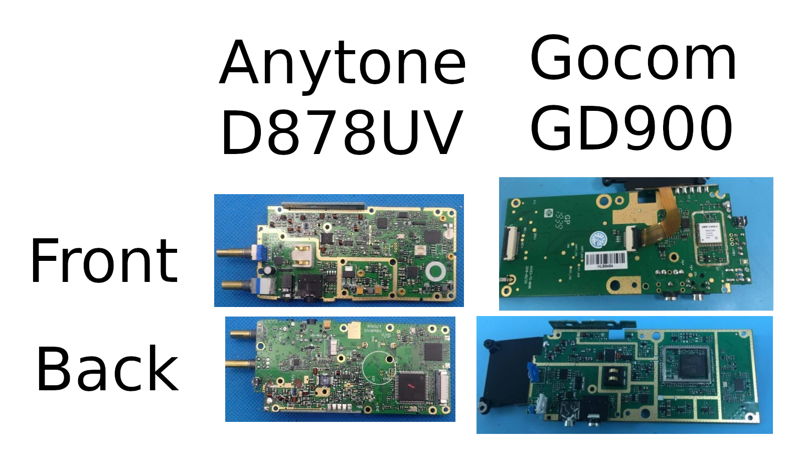 Take a look at the Anytone D878UV vs the GOCOM GD900. Even without
looking in depth, it is clear that the GOCOM radio has a ton of empty
real estate. Granted, the Anytone does have more components in the RF
stage to handle the two bands, but the number of ICs is less than
half. The back side of the GOCOM radio is almost completely empty.
Take a look at the Anytone D878UV vs the GOCOM GD900. Even without
looking in depth, it is clear that the GOCOM radio has a ton of empty
real estate. Granted, the Anytone does have more components in the RF
stage to handle the two bands, but the number of ICs is less than
half. The back side of the GOCOM radio is almost completely empty.
Background
Previously, I dug through what I could find in press releases and what was available from the FCC filings. From this it looks like the A6 is a SoC composed of at least the CPU, memory, and flash coupled with an RF transceiver and a vocoder.
While the integration can definitely explain why there are few ICs, it isn’t clear to me how exactly this is being achieved.
Custom integrated RF ICs are not cheap or easy to design. While it makes sense for Qualcomm to come up with a new IC for a cell phone or Analog Devices for a high cost radar system, it seems odd that we would be seeing this in a $20 radio. The FCC is pushing commercial users toward higher efficiency protocols, but really how many users and radios are there? Even in this case with these radios. Even if we consider they may have landed a big contract with the Chinese government for police radios, that is maybe 1-2 million radios. Worldwide, for all users, I can’t imagine more than one of these radios per 100 people. That would be 60 million radios.
For comparison, Qualcomm spends about $6 billion per year on R&D to produce around 10 new processors per year. These sell for significantly more, and those development costs are spread over billions of devices.
Now DMR is not that complicated of a protocol. It doesn’t have to implement half a dozen different protocols. No one expects an HT to play the latest android games or take pictures or play videos. But it seems pretty incredible that anyone could justify the engineering cost to make this chip from scratch and then sell it for ¥90.
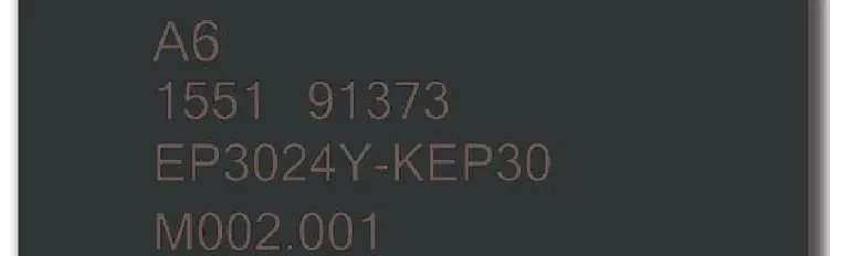
Digging around in the flash
While investigating how the CPS software programs the chip, it became clear that the CPS is reading and writing raw addresses on the chip. Could we learn something by just reading from other memory addresses? The addresses for the reading and writing seemed to be around 0x8200WXYZ, but there were a few in the 0x81e0WXYZ range too. Using the radiodump tool, I poked around in different regions of the memory eventually dumping all of the 81000000 and 82000000 space.
Extracting strings from these dumps, is not too revealing. There are the strings from the codeplug including the channel names and contacts . A few strings are recognizable as command for GPS and Bluetooth devices. But the only string that stood out was a debug message:
|
|
First break
Googling this string leads to several webpages about the Ai-Thinker A9 and A9G GPRS module.
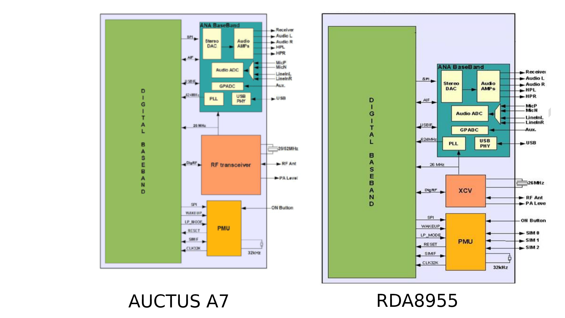
Internally, this module uses the
RDA8955
SoC. The block diagram from the datasheet looks remarkably similar to
one used in a press release
from Auctus. Additionally, the specs seem to be a
very close match with the same CPU speed (312 MHz) and memory (32 Mb
Flash and psRAM).
Memory map
Working off the assumption that the A6 is like something from RDA, several RDA datasheets were collected. Based upon the datasheets for the RDA8851 and RDA88X9 and the files in the A9 repository, the RDA chips share several common features.
The memory model of the A6 is broken into 4 segments:
| Name | Address | Size | Description |
|---|---|---|---|
| kuseg | 0x00000000 | 0x80000000 | 2 GB mapped memory, cached |
| kseg0 | 0x80000000 | 0x20000000 | 512 MB unmapped, cached |
| kseg1 | 0xa0000000 | 0x20000000 | 512 MB unmapped, uncached |
| kseg2 | 0xc0000000 | 0x40000000 | 1 GB mapped, cached |
Within these segments these regions seemed the most promising
| Name | Address | Size | Desc |
|---|---|---|---|
| External RAM | 0x02000000 | 0x02000000 | External shared psRAM |
| External Flash | 0x08000000 | 0x08000000 | External NVM flash |
| XCPU ROM | 0x01e00000 | 0x5000 | Main CPU ROM |
| BCPU ROM | 0x01e80000 | 0x20000 | Baseband CPU ROM |
| XCPU RAM | 0x01ac0000 | 0x20000 | Main CPU internal SRAM |
| BCPU RAM | 0x01980000 | 0x8000 | BCPU internal SRAM |
Both the flash and the ROM have debug strings referencing RDA 8809. Additionally, there are references to SIM card handling in the flash which would seem unlikely in a DMR chip designed from the ground up. Regardless, having these 8809 debug messages in the ROM seems that the A6 is at least a derivative of the RDA 8809.
RDA, AUCTUS and GOCOM
Lets take a step back and see if it makes sense that the A6 might be an RDA8809. RDA and AUCTUS have been in business with each other since 2007 developing RF chips. Notable among the chips is the RDA1846 aka AT1846 series of transceiver ICs found in the Baofeng radios.
In 2014, RDA and AUCTUS divided their respective businesses with RDA focusing on mobile phone products and AUCTUS focusing on private network devices aka walkie-talkies. As part of the agreement, RDA granted licenses to AUCTUS for the MIPS IP as well as manufacturing rights to the RDA1846S(Single chip transceiver), RDA1847(Single chip transceiver), RDA8809(2G GSM transceiver), RDA5891(Chinese TV demodulator), and RDA5590P(WIFI/BT/FM radio) chips. This is probably why the RDA1846 was replaced with the AT1846 around this time. Additionally, they can use several other RDA chips with a licensing fee.
Their agreement allows Auctus to produce derivative chips from all of the licensed technology.
Finally, GOCOM(環球佳美科技有限公司) is the buyer of these new chips and is specifically referenced as one of the main buyers of these chips in regulatory filings. They are responsible for turning the raw chips into modules or devices. These devices are then sold directly to consumers or are produced for other brands. For example, the FCC filing for the COTRE CO01D shows it is a rebrand of a GOCOM GD501 radio.
What is the Auctus A6
I think the A6 is an RDA8809 or some derivative of it. There are references in the ROM to the RDA8809, the memory map seems to match, the CPU architecture is a match and many of the hardware specs align. However, in terms of software, the two are quite far apart.
If the A6 is a derivative of the 8809, the block diagram for the A6 might look like this:
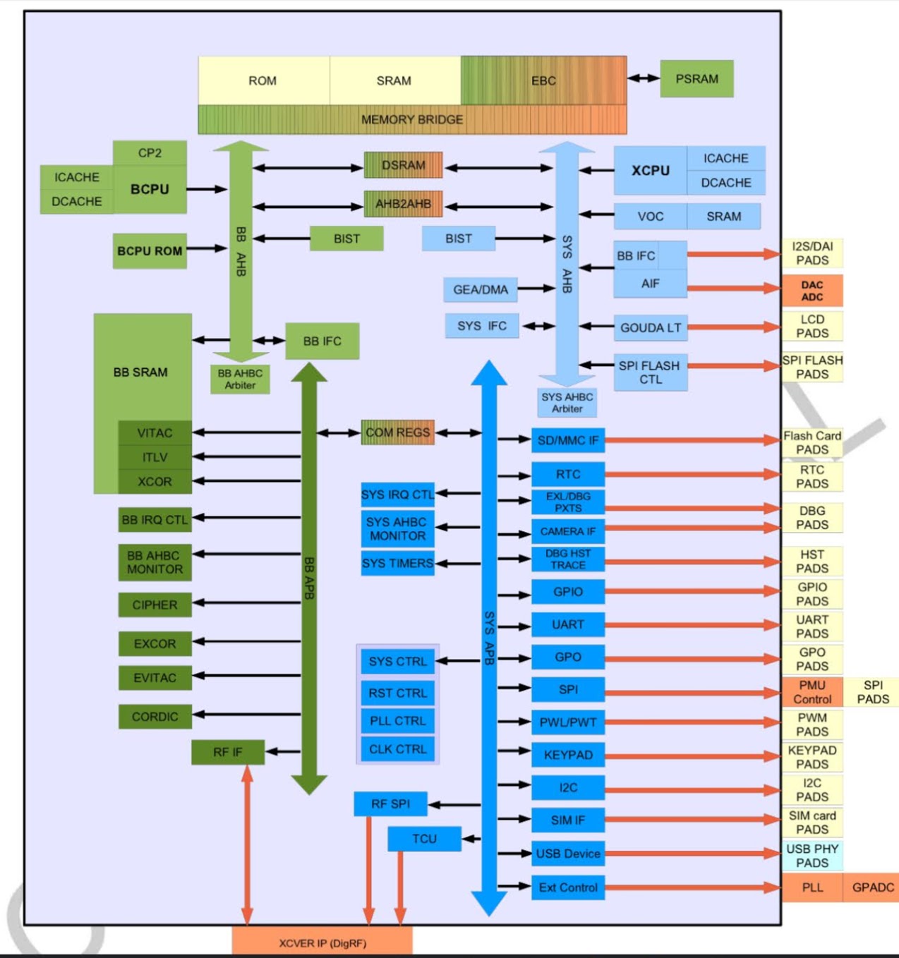
Now there are a lot of different things going on in this chip. There are two general purpose CPUs. BUT they probably should not be considered two cores. Instead they have their own busses with their own peripherals.
The architecture is MIPS and the data sheets from RDA seem to indicate that it is MIPS32 with MicroMIPS instructions, little endian.
XCPU
The XCPU (blue side) runs the frontend. Practically all of the external IO goes through this side. To this CPU we have UARTs, GPIO, USB, keypads, LCD, etc.
BCPU
The BCPU (green side) controls the RF side of things. Think of it as a dedicated SDR. This side takes the I/Q samples and goes through the decoding and eventually sends the data to the XCPU side for output. It has to be encoded data as the vocoder is attached to the XCPU bus. Rather than being a second core and running general routines, the BCPU is a dedicated base band processor. The primary peripheral is the RFSPI IF DAC.
Busses and bridging
The XCPU and BCPU each have two busses. The AHB busses are for high speed communication between the CPU, RAM, ROM and FLASH. The APB bus is slower and communicates with peripherals.
Bridging the two CPUs is a memory bridge where the “external” memory allows for both CPUs to access data. Fast communication can be achieved through the DSRAM mailbox.
Memory
The memory map for the 8809 is likely close to correct for the A6.
It appears that everything which is mapped to a memory address is accessible by any other device in the chip. The debug interface is attached to the XCPU, but the SRAM of the BCPU can be read through this interface.
What does all this mean?
Custom firmware should be a possibility for these radios. Other RDA8809 devices have had custom firmware made for them. We are very fortunate that the CPS programs these radios through a debug interface for the CPU. Based upon other RDA MIPS chips, these radios should be able to be flashed using Cooltools. And beyond that, this interface even allows the gdb to be used.
The tricky part is that the RF interface for this radio is a complete blackbox without some sort of datasheet or sample code. In the ROM and flash there are machine code implementations and there are numerous debug messages which help to identify the functions and their purpose. However for the moment it isn’t even clear where the registers for the RFSPI might exist in memory.
But on the user interface side of things, there exist libraries and headers for the RDA8809 and even some sample applications as a result of the AI Thinker repository. If the ROM isn’t different between the RDA8809 and Auctus A6, it might even be possible to use the AI Thinker A9 to make an FM and/or DMR module.